
Catenaa, Saturday, December 27, 2025-Researchers from Stanford, Carnegie Mellon, Penn, MIT, and SkyWater Technology unveiled the first monolithic 3D computer chip produced in a US foundry recently.
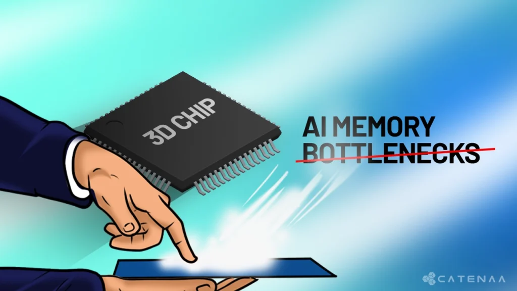
They said that the chip was designed to overcome long-standing AI performance limits known as the “memory wall.”
The prototype stacks ultra-thin layers of memory and processing vertically, enabling data to move far faster between storage and compute elements compared with conventional 2D chips.
The chip integrates multiple layers in a single, continuous fabrication process, rather than stacking separate chips, allowing dense vertical wiring that reduces bottlenecks.
Early tests show the design already outperforms comparable 2D chips by roughly four times, with simulations indicating future iterations could achieve up to twelve-fold gains on AI workloads.
The architecture also improves energy efficiency, with projections for 100- to 1,000-fold improvements in energy-delay product through reduced data movement and greater parallelism.
This achievement marks a first for domestic manufacturing, demonstrating that advanced 3D architectures can be built at commercial scale in the US Researchers emphasize the long-term impact on AI hardware, asserting that tightly integrated 3D designs enable higher throughput, lower energy usage, and faster innovation cycles.
The development addresses the persistent “memory wall,” where data transfer speeds between memory and processing units lag behind computing capacity, a limitation that has slowed AI system advancement.
By combining memory and computation vertically, the chip dramatically shortens data pathways and opens new possibilities for high-performance AI hardware.
The research was supported by DARPA, the U.S. National Science Foundation, Samsung, and other partners, and was presented at the 71st IEEE International Electron Devices Meeting.